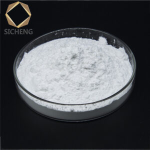
Platelet Calcined Alumina precision lapping for silicon
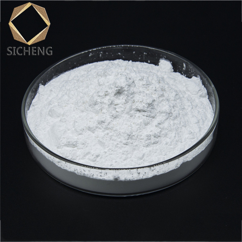
PWA is a precisely graded a-type alumina abrasive powder consisting of a plate-shaped crystal of Al2O3 with a purity of over 90%. With a tremendous range of utilizations, PWA is an abrasive powder capable of performing a myriad of functions.
- Chemically inert
- Will not be corroded by either acids or alkalines
- Excellent heat-resistant properties
- Greater number of uniform grades than available from most manufacturers
The particle size distribution is tightly controlled and produces a very fine lapped surface allowing a wide range of applications, such as:
- Lapping agent for:
- Silicon
- Optical materials
- Liquid crystal
- Stainless steel
- Other materials
- Filler material for coatings
- Material for lapping cloth or paper
- Compounding agent combined with a metal or synthetic resin
| Particle Size | Particle Distribution (µm) | Notes | |||
| Maximum Particle Size | Particle Size at d03 | Particle Size at d50 | Particle Size at d94 | ||
| 45 | < 82.9 | 53.4 ± 3.20 | 34.9 ± 2.30 | 22.8 ± 1.80 | Discontinued |
| WCA40 | < 77.8 | 41.8 ± 2.80 | 29.7 ± 2.00 | 19.0 ± 1.00 | |
| WCA35 | < 64.0 | 37.6 ± 2.20 | 25.5 ± 1.70 | 16.0 ± 1.00 | |
| WCA30 | < 50.8 | 30.2 ± 2.10 | 20.8 ± 1.50 | 14.5 ± 1.10 | |
| WCA25 | < 40.3 | 26.3 ± 1.90 | 17.4 ± 1.30 | 10.4 ± 0.80 | |
| WCA20 | < 32.0 | 22.5 ± 1.60 | 14.2 ± 1.10 | 9.00 ± 0.80 | |
| WCA15 | < 25.4 | 16.0 ± 1.20 | 10.2 ± 0.80 | 6.30 ± 0.50 | |
| WCA12 | < 20.2 | 12.8 ± 1.00 | 8.20 ± 0.60 | 4.90 ± 0.40 | |
| WCA9 | < 16.0 | 9.70 ± 0.80 | 6.40 ± 0.50 | 3.60 ± 0.30 | |
| WCA5 | < 12.7 | 7.20 ± 0.60 | 4.70 ± 0.40 | 2.80 ± 0.25 | |
| WCA3 | < 10.1 | 5.20 ± 0.40 | 3.10 ± 0.30 | 1.80 ± 0.30 | |
For semiconductor materials such as semiconductor silicon wafers, the application of plate aluminum oxide can reduce the grinding time, greatly improve the grinding efficiency, reduce the loss of the grinding machine, save labor and grinding costs, and increase the grinding pass rate. The quality is close to well-known foreign brands.
The work efficiency of the glass bulb grinding of the picture tube is increased by 3-5 times;
The qualified product rate is increased by 10-15%, and the qualified product rate of semiconductor wafers reaches more than 99%;
Grinding consumption is 40-40% less than ordinary alumina polishing powder;
Chemical composition Supply (Platelet Calcined Alumina precision lapping for silicon)
| Al2O3 | ≥99.0% |
| SiO2 | <0.2 |
| Fe2O3 | <0.1 |
| Na2O | <1 |
Physical properties
| Material | α-Al2O3 |
| Color | White |
| Specific gravity | ≥3.9g/cm3 |
| Mohs’Hardness | 9.0 |
Product application range:(Platelet Calcined Alumina precision lapping for silicon)
1) Electronics industry: grinding and polishing of semiconductor monocrystalline silicon wafers, quartz quartz crystals, compound semiconductors (crystalline gallium, phosphating nano).
2) Glass industry: grinding and processing of crystal, quartz glass, kinescope glass shell screen, optical glass, liquid crystal display (LCD) glass substrate, and quartz crystal.
3) Coating industry: special coatings and fillers for plasma spraying.
4) Metal and ceramic processing industry: precision ceramic materials, sintered ceramic raw materials, high-grade high-temperature coatings, etc.
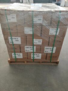
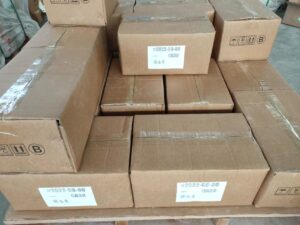
Package:10kgs/bag,20kgs/ Carton
